

I call this my "Lockbox Synth" because the case is made out of an old lockbox. I wanted something very portable, and no CEM's!
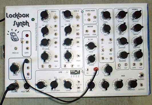 |
| Photos! |
12/22/2002
I corrected a couple of shortcomings of the Lockbox Synth discovered after playing it a while.
| Status |
|
VCO |
|
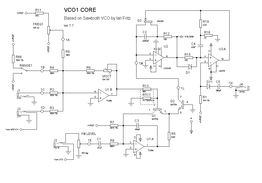
The core of the VCO is the common ASM-1 type sawtooth relaxation oscillator. This one is based on a circuit by
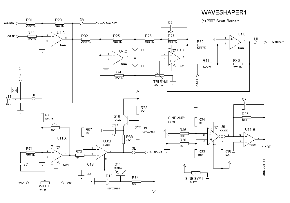
Ian Fritz. Waveshapers provide Triangle, width modulated Pulse,
and Sine waveforms, selectable by a rotary switch. The selected output feeds channels 1 and 2 of the mixer.
I used a range switch rather than a Coarse Frequency knob. It's a center off DPST that adds a negative, 0, or positive offset to the control voltage. CV1 defaults to the output of the Glide Circuit but can be overridden with a patch cord. Schematic of VCO core Waveshapers Theory of Operation |
4 pole LP/BP VCF |
|
The VCF gives switchable 4 pole Lowpass or Bandpass response. The input comes from the Mixer, and the output goes to VCA1.
It is the vcf12a circuit from EFM, with some mofifications. I replaced the exponential generator circuitry, and replaced the Q pot with a dual pot configured as a reverse log pot. |
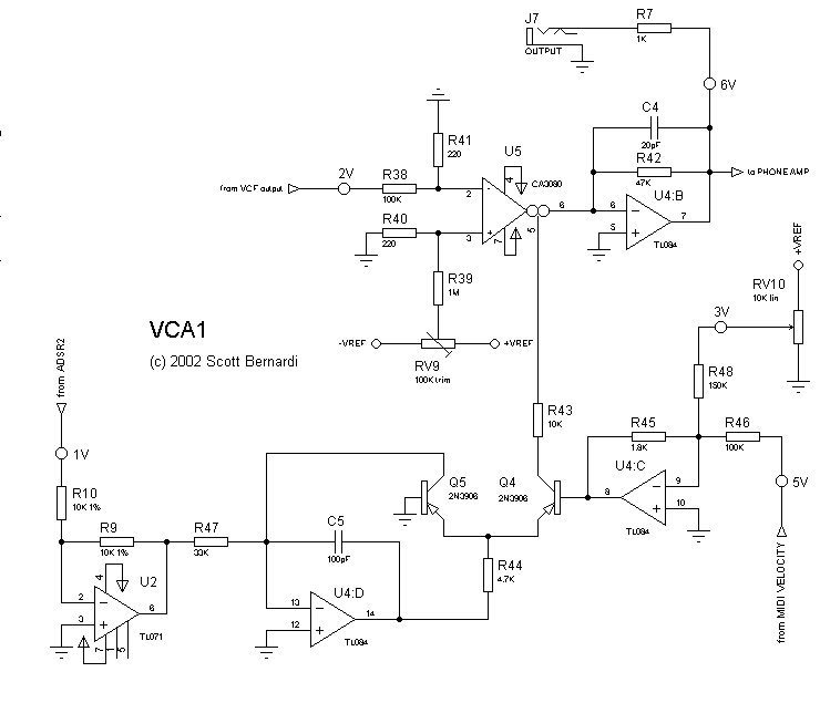
VCA's |
|
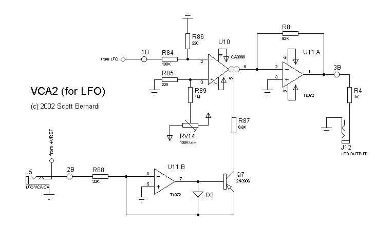
There are two VCA's. VCA2's input is hardwired to the LFO output, and the CV input by default is wired to "full on". This can be overridden
by plugging a patch cord into the VCA CV input, for example hooking it to the Mod CV (MIDI Mod CV wheel) output jack.
VCA1 has both linear and exponential inputs. The linear CV input is hardwired to the ADSR1 output. The exponential CV input is hard wired to the MIDI Velocity control voltage. This is how touch sensitivity is produced. VCA2 linear VCA schematic VCA1 linear/exponential VCA schematic Theory of Operation |
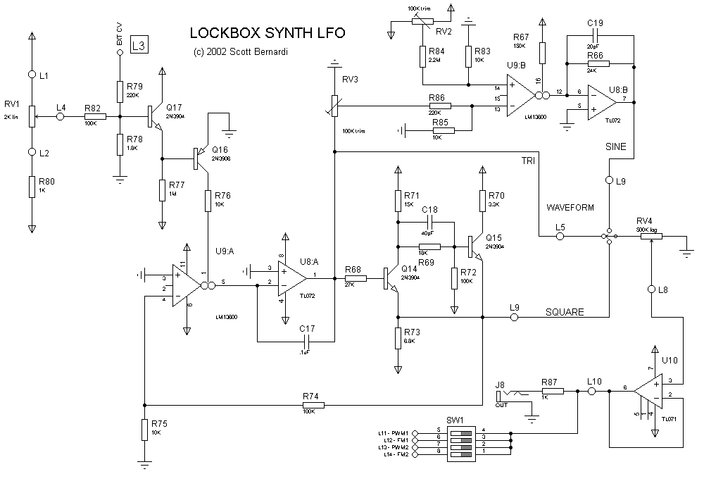
LFO |
|
The LFO has triangle, sine, and square outputs, a level control, and dedicated VCA. Switches
connect the output to the PWM inputs of FM inputs of VCO1 and/or VCO2.
LFO schematic Theory of Operation |
Noise Source |
| The noise source is just an amplified reversed biased transistor BE junction. I used a 2N2712 'cuz it was the noisiest transistor
I had on hand. Outputs are White and Pink noise. The White Noise output also feeds channel 3 of the mixer, the Pink noise feeds the
default input of the Sample & Hold (overridable).
I originally had the white noise feeding the S&H, but the Rate pulse from the S&H was feeding into the noise, causing voltage spikes (you could hear them as "pops"), which in turn affected the S&H output levels. You have to be real careful with high gain circuits like the noise source. The Noise Source and S&H were on the same PCB, but had totally separate power supply connections. It's interesting that when I hooked the Pink noise output into the S&H input, it not only cleaned up the S&H output, but also the white noise output had no more spikes! ("Clean" noise?) Noise schematic |
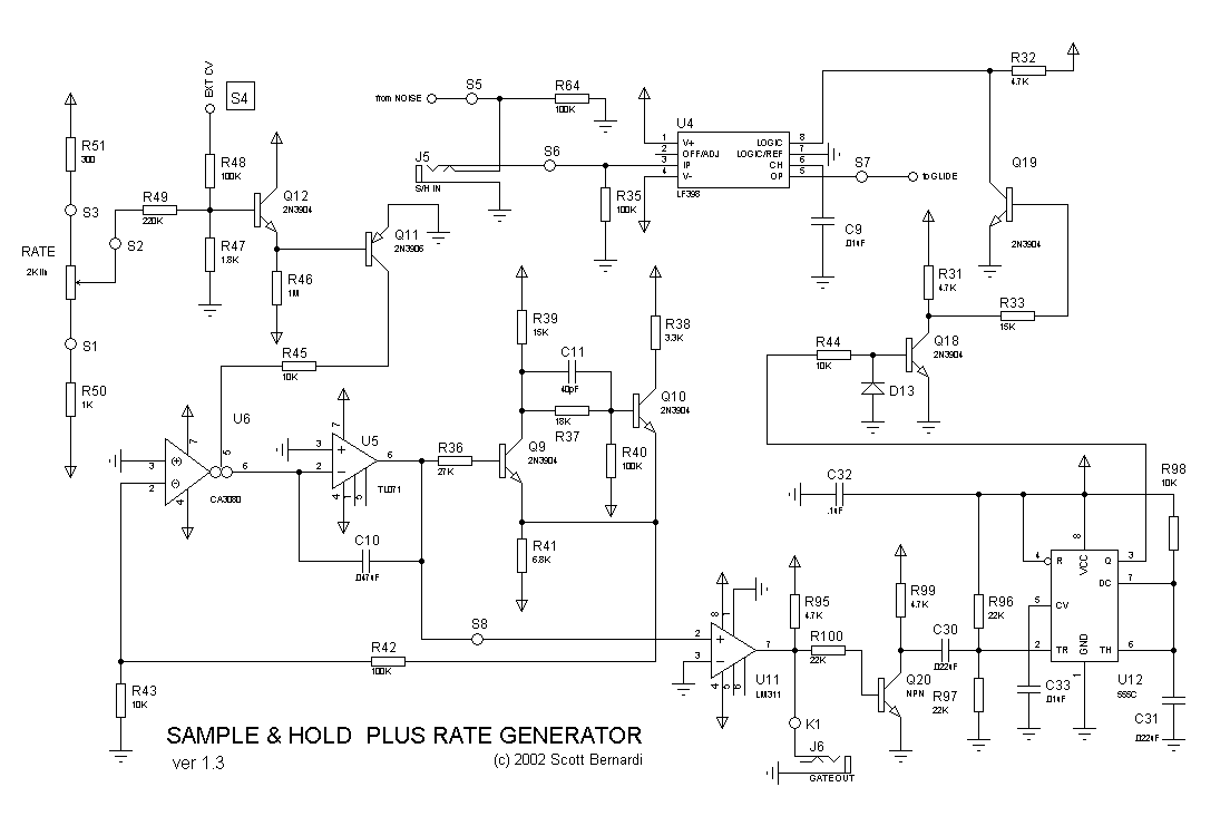
Sample and Hold |
| The Sample and Hold has a dedicated Rate oscillator and Glide circuit. I used the National LF398 IC for the actual S&H.
The input defaults to the Pink Noise output, but can be overridden with a patch cord.
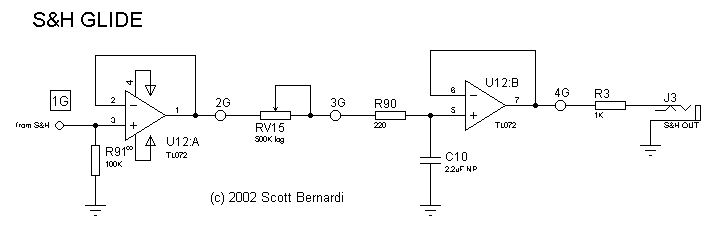
In retrospect, I should have provided a GATE OUT jack from the LFO square output to be used to drive the ADSRs when using the S&H as the control voltage source. I ended up adding a switch near the GATE OUT multiples where the MIDI GATE or the S&H GATE could be routed to the multiples and the internal ADSR connections. Sample and Hold Schematic Theory of Operation Glide for S&H |
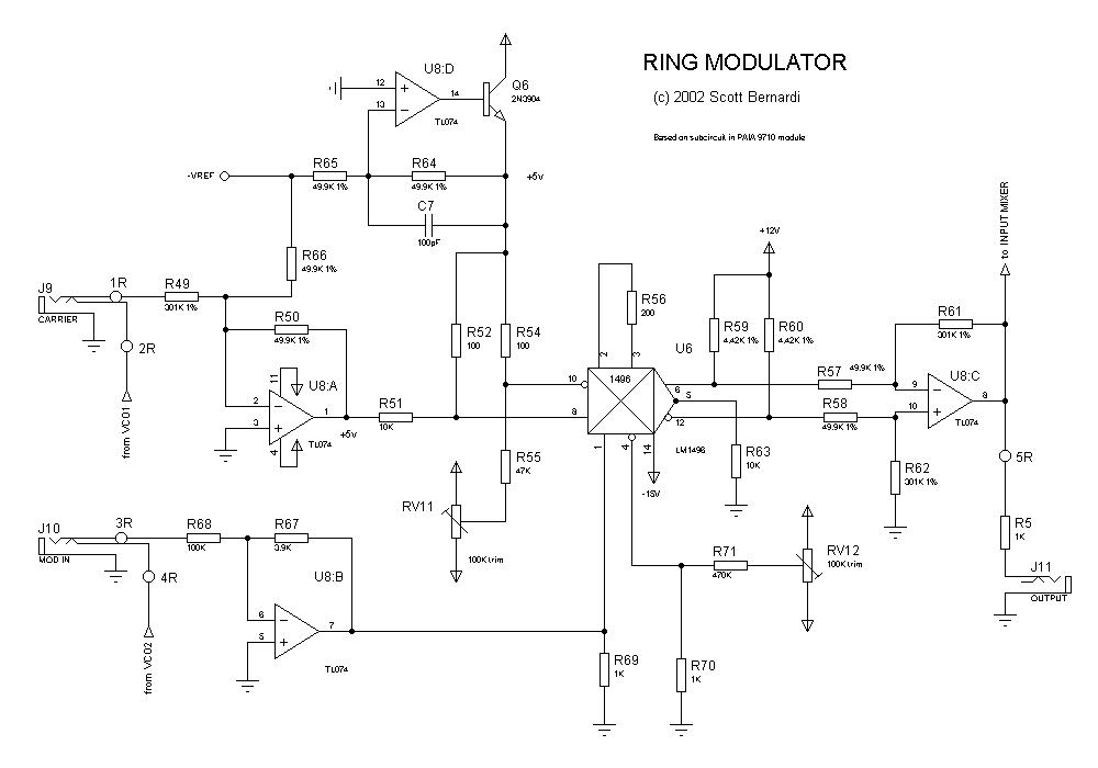
Ring Modulator |
| The ring modulator circuit uses the MC1496 balanced modulator IC. It's the same circuit I used in og2. The default inputs are
VCO1 and VCO2, overridable with a patch cord. The output feeds the mixer.
Ring Modulator Schematic Theory of Operation |
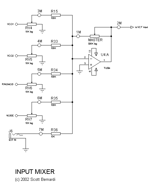
Mixers |
| The mixer has hardwired inputs from VCO1, VCO2, the Ring Modulator, Noise, and an External Input jack. The hardwired
inputs each have input attenuators, and an maximum gain of 5 (set by Master Gain pot). The External Input has a maximum gain of 50
and no input attenuator. The output of the mixer feeds the VCF.
Mixer schematic |
Midi 2 CV |
| The Midi 2 CV module is the RXCV-Pro from EFM. This module has v/octave (keyboard), pitchbend, velocity, and Mod control voltages, and Key Gate and Glide gate. |
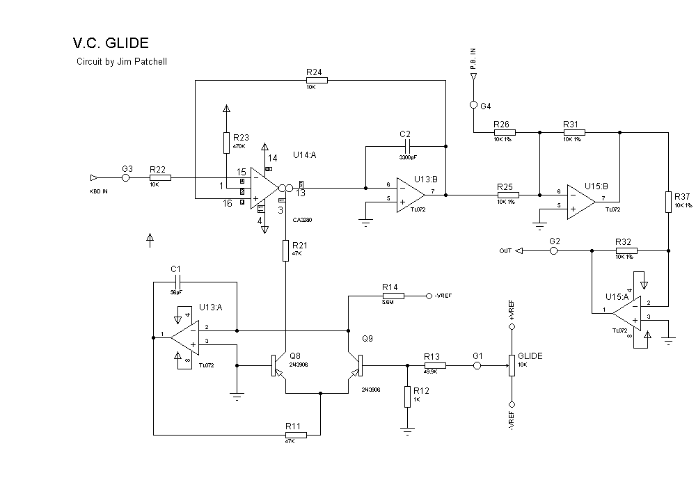
Voltage Controlled Glide |
| This is a circuit from Jim Patchell. I was originally going to use the S&H Glide circuit, but if you use a big enough pot to get real long delay times, the resolution
at the very important short delay times is lousy. A voltage controlled Glide/Portamento circuit solves this problem.
V.C. Glide schematic Theory of Operation |
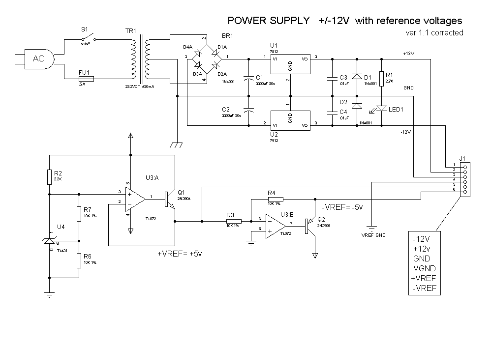
Power Supply |
| Power supplies are pretty mundane, but you gotta have 'em. Mine is a +/-12v 7812/7912 based, with temperature
stable +/-5v reference voltages. I used a TL431 voltage reference chip which I buffered with an opamp and pass transistor, just because I scored a bunch
of them cheap on eBay.
I used 6 pin headers and connectors (-V, +V, GND, RefGND, +Vref, -Vref). The arrangement of the voltages means I could even plug the connector in backwards and it wouldn't blow anything. Power Supply Schematic |