
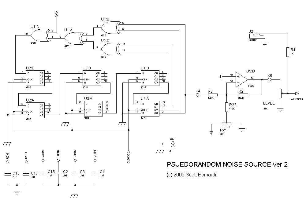
Transistor noise sources require high gain to amplify the noise from a reverse biased pn junction. I've had problems with crosstalk from
other circuits (for eample, on my Lockbox synth, you can hear a bit of the VCO's in the noise). This digital pseudorandom noise source
circuit does not have that problem, and also provides a stable peak to peak output.
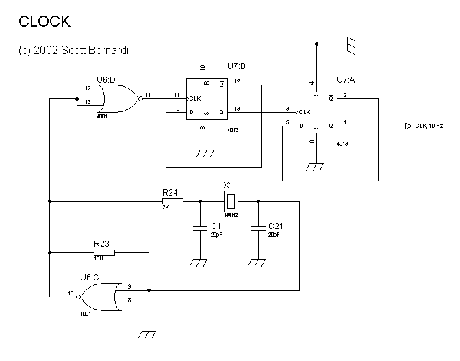
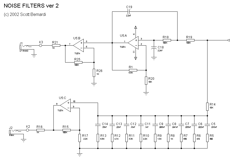
Pseudorandom Noise schematic How it worksA Linear Feedback Shift Register pseudo-random noise circuit uses cascaded recirculating shift registers with modulo-2 (XOR) feedback from certain taps. I used 24 bits (three 8 bit shift registers) with taps at bit 17, 22, 23, and 24, according to theory. This produces a repeatable sequence of 2^n-1, or 16,777,215 states. The circuit is clocked at 1MHz, so the cycle repeats in about 17 seconds - too slow to be noticable.Originally I had the output of the PRNG capacitively coupled at a low frequency to the Pink and LF Random filters. But this caused problems when the Level was adjusted - the low time constant cause the Pink and LF Random outputs to bang into the rails temporarily, then drift back down into the linear region. So I added an opamp inverting summer to provide some gain and to add in an offest to trim out the 2.5v DC bias prior to the Level control, and dc coupled the following stages. The clock circuit is a standard crystal oscillator. A twin-T oscillator tuned to the crystal frequency 1/(2*PI*2K*20pF) ~ 4MHz is placed in the feedback loop of an amplifier. The amplifier is made by biasing a CMOS inverter (U6:B) in its linear region with a 10M resistor. The output is buffered with another inverter U6:D. Since I actually wanted 1MHz, the frequency is divided down with two flip-flops U7. |