
| Status |
|
|
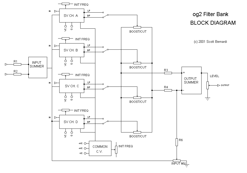
Warning! If you picked up the schematics prior to 08/30/2002, get a new copy! Mistakes have been corrected. Version should say 2.1 Here we present a four channel voltage controlled filter bank. Referring to the block diagram, an input summer summs (and inverts) the inputs and feeds them simultaneously to all four filter channels. The filter channels are voltage controlled state variable types with independently adjustable fc and Q. In addition, a common control voltage is sent to each filter. This way the channels may have their initial frequencies set independently, and the whole filter bank made to track a keyboard. The Q controls are voltage controlled also. Any of the three filter responses may be selected. They are configured like an equalizer, where the channel's output can be added or subtracted (boost or cut) from the input signal via the Boost/Cut controls. The outputs of the filter channels are summed in the output summing amp. Also, all or a portion of the input signal can be added also, as determined by the Input Mix control. |
The arrangement presented provides a lot of flexibility.
|
V.C. State Variable Filter schematic
The voltage controlled state variable filter is a fairly standard one with simultaneous BP, LP, and HP outputs OTA U3:A forms the basis for voltage controlled Q. Boost/Cut functionality is achieved by summing a non-inverted or inverted signal into the Master Mixer circuitry. |
Frequency and Q control voltage circuits
Exponential current sources for the OTA's are shown here. These circuits will be repeated for each of the filter channels. The frequency control exponential current source is temperature compensated. Since the filter channel will double as a sine wave VCO, I wanted them to be more stable than a VCF usually requires. Q1, Q2, and TC1 should be in thermal contact. Q1 and Q2 are a matched pnp pair. Since matched pnp transistors are pretty hard to find, I hand match a pair of 2N3906's for Vbe. The frequency control has VC inputs labeled "CV", "Formant CV", "Master CV", "Var CV", and the Initial Frequency pot.
|
Master Mix schematic
Master Frequency CV schematic
Circuity common to all channels includes:
|